Module Patch Plug-in Processing

In PCBA processing, with the chip processing equipment more and more powerful, PCB and electronic components are becoming smaller and smaller, SMT chip processing is becoming more and more popular, chip processing gradually replace the previous plug-in processing. But some circuit boards still need plug-in processing, plug-in processing in the current electronic processing industry is still very common, DIP plug-in processing in the SMD processing is completed.

Order Quantity ≥1PC
Quality Grade IPC-A-610
Min Package 01005 (0.4mm*0.2mm)
Processing Technology Electrolytic Foil

Prototype to Full Turn-Key Assembly

Through-Hole Lead-Free Wave Soldering

Best Price, Genuine Components

Quality Accreditation ISO9001

  • Description
  • Specification

DIP Plug-in Process Flow Introduction

In PCBA processing, with the chip processing equipment more and more powerful, PCB and electronic components are becoming smaller and smaller, SMT chip processing is becoming more and more popular, chip processing gradually replace the previous plug-in processing. But some circuit boards still need plug-in processing, plug-in processing in the current electronic processing industry is still very common, DIP plug-in processing in the SMD processing is completed.Dual In-line Package, also known as dual in-line package technology, refers to the use of dual in-line package form of integrated circuit chips, the vast majority of small and medium-sized integrated circuits are using this package form, the number of pins generally does not exceed 100

1. BOM checklist, scheduling process

Receive materials according to the BOM bill of materials, check the material type and specification, then arrange the process and assign components for each job

2. Plug-in

Insert the components that need to pass through the hole to the corresponding position of PCBA board, in preparation for wave soldering.

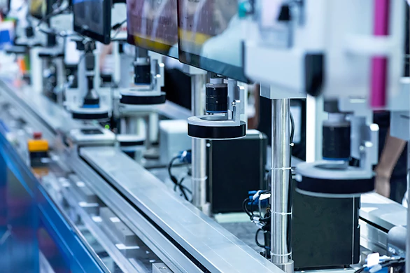
3. Wave soldering machine

Put the plug-in PCBA board into the wave soldering conveyor belt, after spraying flux, preheating, wave soldering, cooling and other links, to complete the wave soldering of PCBA board.

4. Components cutting foot

The finished PCBA board is cut to the right size.

5. Post-soldering

For checking out the finished PCBA board that is not soldered completely should be made up and repaired.

6. Wash the board

Clean the residual flux and other harmful substances on the finished PCBA to achieve the environmental standard cleanliness required by the customer.

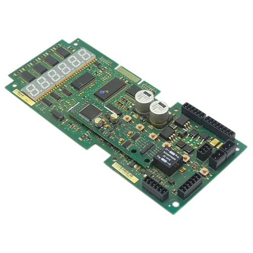
7. Testing/quality inspection

After the components are soldered, the finished PCBA products should be tested for functionality, to test whether the functions are normal and to ensure that the products are delivered to customer satisfaction.

ltem Capability
Order Quantity ≥1PC
Quality Grade IPC-A-610
Lead Time 24 hours expedited service can be offered. 3- 4 days normally for PCBA prototype orders. We will give you an accurate lead time when we quote for you.
Size 50*50mm~510*460mm
Board Type Rigid PCB, Flexible PCB, metal core PCB
Min Package 01005 (0.4mm*0.2mm)
Max Package No limit
Mounting Accuracy ±0.035mm(±0.025mm)  Cpk≥1.0 (3σ)
Surface Finish Lead/Lead-free HASL, Immersion gold, OPS, etc.
Assembly Types Surface mount (SMT), Through-hole (DIP), Mixed Technology (SMT & Thru-hole)
Component Sourcing Turnkey (All components sourced by Wenshu), Partial turnkey, Kitted/Consigned
BGA Package BGA Dia. 0.14mm, BGA 0.2mm pitch
SMT Parts Presentation Cut Tape, Partial reel, Reel, Tube, Tray, Laser-cut Stainless Steel
Cable Assembly We supply custom cables, cable assemblies, wiring looms/harnesses and power leads for various industries including automotive, security, mining, medical and entertainment.
Stencil Stencil with or without frame (offered free by Wenshu)
Quality Inspection Visual inspection; AOI checking; BGA placement – X-RAY checking
SMT Capacity 3 Million~4 Million Soldering Pad/day
DIP Capacity 100 Thousand Pins/day

Our Solution for High Quality Printed Circuit Boards and Precision Product Assembly