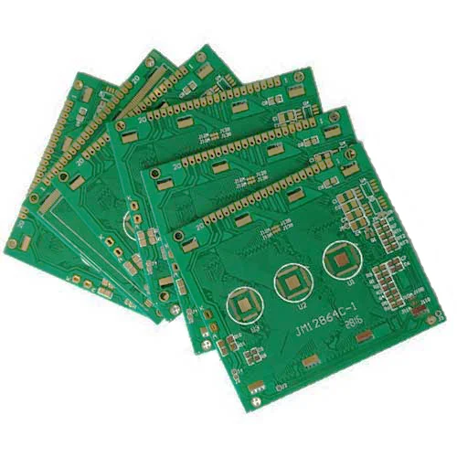
LCD Liquid Crystal Display PCB Assembly
LCD liquid crystal display PCB circuit board – liquid crystal display, that is the display. LCD is a typical three-layer structure in which the liquid crystal is placed between two parallel sheets of glass. There are many small vertical and horizontal lines between the two pieces of glass. The direction of the rod-shaped crystal molecules is changed by a voltage, and the picture is also displayed.
| Layers | 2L |
| Plate thickness | 1.6mm |
| Size | 147.2*65mm |
| Minimum aperture | 0.22mm |
| Line width/moment | 0.3*0.27mm |
| Surface treatment | lead-free spray tin |
Prototype to Full Turn-Key Assembly
Through-Hole Lead-Free Wave Soldering
Best Price, Genuine Components
Quality Accreditation ISO9001
-
Description
-
Specification
Introducing our state-of-the-art LCD Liquid Crystal Display PCB, the perfect solution for all your visual display needs. This advanced PCB module combines cutting-edge technology, superior design, and exceptional performance. It deliver crystal-clear images and an immersive visual experience.
Our LCD Liquid Crystal PCB is meticulously engineered to ensure optimal performance and reliability. With a compact form factor, it seamlessly integrates into various electronic devices, making it an ideal choice for applications such as televisions, computer monitors, digital signage, medical equipment, and more.
LCD liquid crystal display PCB circuit board – liquid crystal display, that is the display. LCD is a typical three-layer structure in which the liquid crystal is placed between two parallel sheets of glass. There are many small vertical and horizontal lines between the two pieces of glass. The direction of the rod-shaped crystal molecules is changed by a voltage, and the picture is also displayed.
Upgrade your visual displays with our advanced LCD Liquid Crystal PCB and elevate your viewing experience to a whole new level. Whether you’re a professional seeking high-performance display for your projects or an individual looking to enhance your entertainment setup, our PCB module delivers exceptional quality, reliability, and versatility. Choose excellence in visual technology with our LCD Liquid Crystal Display PCB.
| ltem | Capability |
|---|---|
| Layer Count | 1-40layers |
| Base Material | KB、Shengyi、ShengyiSF305、FR408、FR408HR、IS410、FR406、GETEK、370HR、IT180A、Rogers4350、Rogers4000、PTFE Laminates(Rogers series、Taconic series、Arlon series、Nelco series)、Rogers/Taconic/Arlon/Nelco laminate with FR-4 material (including partial Ro4350B hybrid laminating with FR-4) |
| Board Type | Backplane、HDI、High multi-layer blind&buried PCB、Embedded Capacitance、Embedded resistance board 、Heavy copper power PCB、Backdrill, PCB Gold Finger |
| Board Thickness | 0.2-5.0mm |
| Copper Thickness | Min. 1/2 OZ, Max. 10 OZ |
| PTH Wall | 25um(1mil) |
| Maximum Board Size | 1100*500mm(43”*19”) |
| Min laser drilling size | 4mil |
| Min.spacing/Tracing | 2.7mil/2.7mil |
| Solder Mask | Green, Black, Blue, Red, White, Yellow, Purple matte/glossy |
| Surface Treatment | Flash gold(electroplated gold)、ENIG、Hard gold、Flash gold、HASL Lead-free 、OSP、ENEPIG、Soft gold、Immersion silver、Immersion Tin、ENIG+OSP, ENIG+Gold finger, Flash gold(electroplated gold)+Gold finger(50u”), Immersion silver+Gold finger, Immersion Tin+Gold finger |
| Min. Annular Ring | 3mil |
| Aspect ratio | 10:1(HASL Lead-free 、HASL Lead、ENIG、Immersion Tin、Immersion silver、ENEPIG);8:1(OSP) |
| Impedance control | ±5ohm(<50ohm), ±10%(≥50ohm) |
| Other Techniques | Blind/Buried Via, Gold Fingers, Press Fit, Via in Pad, Electrical Test |


