Double-Sided Gold Finger Circuit Board Assembly
Gold fingers are the gold-plated posts you see on the edge of a printed circuit board Assembly (PCBA) connection. The purpose of the golden finger is to connect the auxiliary PCB assembly to the motherboard of the computer. PCB assembly gold fingers are also used in various other devices that communicate via digital signals, such as consumer smartphones. Gold is used for connection points along the PCB assembly due to the alloy’s excellent electrical conductivity.
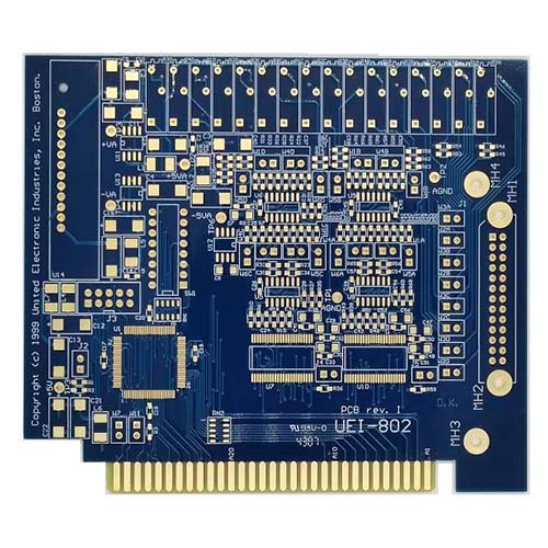
| Layers | 2L |
| Plate thickness | 1.6mm |
| Minimum aperture | 0.3mm |
| Line width | 0.15mm |
| Line distance | 0.15mm |
| Surface Treatment | Immersion Gold |
Prototype to Full Turn-Key Assembly
Through-Hole Lead-Free Wave Soldering
Best Price, Genuine Components
Quality Accreditation ISO9001
-
Description
-
Specification
Double-sided gold finger circuit board Gold-finger PCBs are those with gold-finished finger-like pads that are typically used as edge connectors.
Electroless gold has excellent solderability, but the chemical deposition process means it is too soft and thin to withstand repeated wear and tear. Gold plating is thicker and harder, making it ideal for re-mating PCB edge connector contacts.
Gold finger PCBs also often have to be chamfered at the edge connectors to ensure easy insertion. Bevel cuts can be specified in the order details if specifically stated.
Gold fingers are the gold-plated posts you see on the edge of a printed circuit board (PCB) connection. The purpose of the golden finger is to connect the auxiliary PCB to the motherboard of the computer. PCB gold fingers are also used in various other devices that communicate via digital signals, such as consumer smartphones. Gold is used for connection points along the PCB due to the alloy’s excellent electrical conductivity.
Kinds of gold suitable for PCB gold finger plating process
There are two kinds of gold suitable for PCB gold finger-plating process:
Electroless Nickel Immersion Gold (ENIG): This gold is more cost-effective and easier to solder than electroplated gold, but its soft, thin (typically 2-5u” composition makes ENIG unsuitable for circuit board insertion and removal wear and tear Effect.
Electroplated hard gold: This gold is solid (hard) and thick (usually 30u”), so it is more suitable for the abrasive effects of continuous use of the PCB.
Gold fingers enable different circuit boards to communicate with each other. From a power source to a device or equipment, a signal must pass between multiple contacts in order to execute a given command.
The gold fingers should not have any contact with the solder mask or silk screen, and the two should be kept at a certain distance.
Double-sided gold finger circuit board must always face opposite the middle of the PCB (if you want the edge beveled)
Gold is used for the connection fingers on the PCB because of the alloy’s excellent strength and electrical conductivity. The strength of the gold allows fingers to be inserted and ejected hundreds of times without fraying the connecting contacts. Without the protection of gold plating, the board can easily lose connectivity after a few uses.
As PCBs evolved into their modern form, gold was determined to be the most suitable connection contact metal due to a number of factors. The main advantages of gold are the electrical conductivity and also corrosion resistance of the alloy. For added strength, gold used in printed circuit boards is often combined with nickel or cobalt. For the electroplating process, the thickness of nickel is between 150 and 200 microinches.
| ltem | Capability |
|---|---|
| Layer Count | 1-40layers |
| Base Material | KB、Shengyi、ShengyiSF305、FR408、FR408HR、IS410、FR406、GETEK、370HR、IT180A、Rogers4350、Rogers4000、PTFE Laminates(Rogers series、Taconic series、Arlon series、Nelco series)、Rogers/Taconic/Arlon/Nelco laminate with FR-4 material (including partial Ro4350B hybrid laminating with FR-4) |
| Board Thickness | 0.2-5.0mm |
| Copper Thickness | Min. 1/2 OZ, Max. 10 OZ |
| PTH Wall | 25um(1mil) |
| Maximum Board Size | 1100*500mm(43”*19”) |
| Min laser drilling size | 4mil |
| Min.spacing/Tracing | 2.7mil/2.7mil |
| Solder Mask | Green, Black, Blue, Red, White, Yellow, Purple matte/glossy |
| Surface Treatment | Flash gold(electroplated gold)、ENIG、Hard gold、Flash gold、HASL Lead-free 、OSP、ENEPIG、Soft gold、Immersion silver、Immersion Tin、ENIG+OSP, ENIG+Gold finger, Flash gold(electroplated gold)+Gold finger(50u”), Immersion silver+Gold finger, Immersion Tin+Gold finger |
| Min. Annular Ring | 3mil |
| Aspect ratio | 10:1(HASL Lead-free 、HASL Lead、ENIG、Immersion Tin、Immersion silver、ENEPIG);8:1(OSP) |
| Impedance control | ±5ohm(<50ohm), ±10%(≥50ohm) |
| Other Techniques | Blind/Buried Via, Gold Fingers, Press Fit, Via in Pad, Electrical Test |