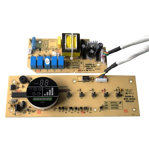
Air Conditioner Controller DIP Processing
Dip package (Dual In-line Package) can also be called dual in-line packaging technology. This refers to the integrated circuit chips that are packaged in dual in-line form during the dip operation of the PCB board manufacturer PCBA. At present, most. The small and medium-sized integrated circuits will use this packaging method, and the number of pins generally does not exceed 100; the CPU chip in the DIP package has two rows of pins, which need to be inserted into the chip socket with the dip structure, or directly Soldering is performed on PCB boards with the same number of solder holes and geometric arrangement.
| Size | 50*50mm~510*460mm |
| Min Package | 01005 (0.4mm*0.2mm) |
| Mounting Accuracy | ±0.035mm (±0.025mm) |
| Processing Technology | Electrolytic Foil |
Prototype to Full Turn-Key Assembly
Through-Hole Lead-Free Wave Soldering
Best Price, Genuine Components
Quality Accreditation ISO9001
-
Description
-
Specification
Dip package (Dual In-line Package) can also be called dual in-line packaging technology. This refers to the integrated circuit chips that are packaged in dual in-line form during the dip operation of the PCB board manufacturer PCBA. At present, most. The small and medium-sized integrated circuits will use this packaging method, and the number of pins generally does not exceed 100; the CPU chip in the DIP package has two rows of pins, which need to be inserted into the chip socket with the dip structure, or directly Soldering is performed on PCB boards with the same number of solder holes and geometric arrangement.
The DIP packaged chip must be carefully inserted and removed from the chip socket to avoid damage to the pins during handling by the SMT technician. DIP package structure forms are: multilayer ceramic double in-line DIP, single-layer ceramic double in-line DIP, lead frame DIP (including glass ceramic sealing type, plastic encapsulation structure type, ceramic low-melting glass encapsulation type) Wait.
Welding after DIP plug-in chip processing is a process after SMT chip processing (except for special cases: only plug-in PCB boards). The processing flow is as follows:
1. Pre-processing PCB components
The staff in the pre-processing workshop will pick up the materials in the material list according to the BOM material list, carefully check the material model and specifications, and then sign, perform pre-processing before production according to the model, and use the automatic bulk capacitor clipper and the transistor to automatically form Machine, automatic belt molding machine and other molding equipment for processing.
Require:
(1) The horizontal width of the adjusted component pins must be the same as the width of the positioning hole, and the tolerance is less than 5%;
(2) The distance between the component pins and the PCB circuit board pads should not be too large;
(3) If the customer requests, the parts need to be formed to provide mechanical support to prevent the pads of the PCB circuit board from lifting.
2. Paste high-temperature adhesive paper, enter the PCB board – paste high-temperature adhesive paper, and block the tin-plated through holes and the components that must be soldered afterwards;
3. The DIP plug-in processing staff must wear an electrostatic wristband to prevent static electricity, and perform plug-in processing according to the component BOM list and component bit number map. The SMT patch processing operator must be careful when plugging in, and there should be no plugs. Mistakes and omissions occur;
4. For the components that have been inserted, the operator must check, mainly to check whether the components are inserted incorrectly or missing;
5. For the PCB board with no problem with the plug-in, the next step is wave soldering, through the wave soldering machine to carry out all-round automatic PCB circuit board soldering treatment, and firm components;
6. Remove the high-temperature adhesive tape, and then perform an inspection. In this link, the main visual inspection is to observe whether the soldered PCB board is well soldered or not;
7. For PCB boards that are not completely soldered, repair soldering and repair to prevent problems;
8. Post welding, this is a process set for specially required components, because some components cannot be directly welded by a wave soldering machine according to the limitations of the process and materials, and they need to be manually completed by the operator;
9. For all the components on the PCB circuit board pads, after the PCB soldering is completed, the PCB board will also need to be processed for functional testing to test whether each function is in a normal state, if the function is checked For defects, the staff must immediately make a mark to be processed, and then repair the PCB circuit board again to test and deal with it.
| ltem | Capability |
|---|---|
| Order Quantity | ≥1PC |
| Quality Grade | IPC-A-610 |
| Lead Time | 24 hours expedited service can be offered. 3- 4 days normally for PCBA prototype orders. We will give you an accurate lead time when we quote for you. |
| Size | 50*50mm~510*460mm |
| Board Type | Rigid PCB, Flexible PCB, metal core PCB |
| Min Package | 01005 (0.4mm*0.2mm) |
| Max Package | No limit |
| Mounting Accuracy | ±0.035mm(±0.025mm) Cpk≥1.0 (3σ) |
| Surface Finish | Lead/Lead-free HASL, Immersion gold, OPS, etc. |
| Assembly Types | Surface mount (SMT), Through-hole (DIP), Mixed Technology (SMT & Thru-hole) |
| Component Sourcing | Turnkey (All components sourced by New Reach), Partial turnkey, Kitted/Consigned |
| BGA Package | BGA Dia. 0.14mm, BGA 0.2mm pitch |
| SMT Parts Presentation | Cut Tape, Partial reel, Reel, Tube, Tray, Laser-cut Stainless Steel |
| Cable Assembly | We supply custom cables, cable assemblies, wiring looms/harnesses and power leads for various industries including automotive, security, mining, medical and entertainment. |
| Stencil | Stencil with or without frame (offered free by New Reach) |
| Quality Inspection | Visual inspection; AOI checking; BGA placement – X-RAY checking |
| SMT Capacity | 3 Million~4 Million Soldering Pad/day |
| DIP Capacity | 100 Thousand Pins/day |