10-Layer 1-Stage HDI Communication PCB Assembly
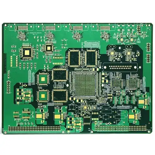
The 10-Layer 1-Stage HDI Communication PCB is an advanced printed circuit board designed specifically for communication applications that require high-density interconnect (HDI) technology. It offers superior signal integrity, increased functionality, and enhanced reliability. This also makes it well-suited for use in telecommunications, networking, and other communication systems.
| Plate thickness | 1.2mm |
| Panel Size | 110.8*94.8mm/4 |
| Minimum blind hole | 0.10mm |
| Minimum BGA | 0.20mm |
| Minimum through hole | 0.20mm |
| Line width and line spacing | 2.5/2.2mil |
Prototype to Full Turn-Key Assembly
Through-Hole Lead-Free Wave Soldering
Best Price, Genuine Components
Quality Accreditation ISO9001
-
Description
-
Specification
The 10-Layer 1-Stage HDI Communication PCB is an advanced printed circuit board designed specifically for communication applications that require high-density interconnect (HDI) technology. It offers superior signal integrity, increased functionality, and enhanced reliability. This also makes it well-suited for use in telecommunications, networking, and other communication systems.
Technical features:
50 Ω Antenna, 90Ω & 100Ω Differential Impedance
Application of 10-layer 1-stage HDI communication PCB:
Cell Phones, Tablets, Ultrabooks, E-Readers, MP3 Players, GPS, Portable Game Consoles, DSCs, Cameras, LCD TVs, POS Terminals
HDI PCB assemblies are widely used to reduce the weight and overall size of products, as well as improve the electrical performance of devices.
HDI PCB assemblies also play an important role in medical equipment as well as various electronic aircraft components. The possibilities for high-density interconnect 10-layer 1-stage communication PCB technology seem almost limitless.
| Feature | Capability |
|---|---|
| Material | FR-4 Standard Tg 140°C, FR4-High Tg 170°C |
| Min. Track/Spacing | For External layers: 4oz Cu 10mil/13mil, 5oz Cu 12mil/15mil, 6oz Cu 15mil/15mil For Internal layers: 4oz Cu 8mil/8mil, 5oz Cu 10mil/10mil, 6oz Cu 12mil/12mil |
| Min. Hole Size | 0.15 ~ 0.3mm |
| Max Outer Layer Copper Weight (Finished) | 12oz |
| Max Inner Layer Copper Weight | 12oz |
| Board Thickness | 0.6-6mm |
| Surface Finishing | HASL lead-free, Immersion gold, OSP, Hard Gold, Immersion Silver, Enepig |
| Solder Mask | Green, Red, Yellow, Blue, White, Black, Purple, Matte Black, Matte green |
| Silkscreen | White, Black |
| Via Process | Tenting Vias, Plugged Vias, Vias not covered |
| Testing | Fly Probe Testing (Free) and A.O.I. testing |
| Build time | 5-15 days |
| Lead time | 2-3 days |